Researchers Uncover Scalable Method for Ultrahigh-Resolution Quantum Dot Displays
Researchers discover universal, nondestructive photolithography method for quantum dot patterning for high-resolution next-generation displays
Colloidal quantum dot (QD) light-emitting diodes have great potential in display applications. However, their commercialization remains a challenge due to the difficulty in achieving high-resolution patterning of QDs without degrading their optical properties. To address this, researchers have developed a nondestructive method for ultrahigh-resolution QD patterning. By blending QDs with a photocrosslinkable polymer, the approach preserves their optical properties and boosts efficiency and lifetime, paving the way for development of next-generation display technologies.

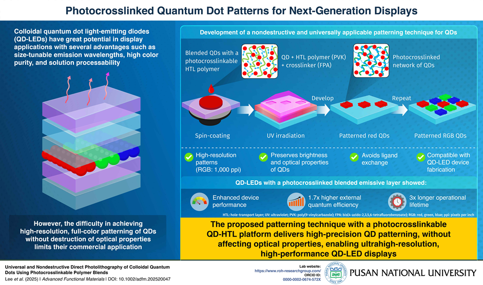
Image title: Photocrosslinked quantum dot (QD) patterns for next-generation displays
Image caption: Researchers develop a nondestructive, universal QD patterning method that blends QDs with a photocrosslinkable hole-transport layer polymer for next-generation display technologies.
Image credit: Dr. Jeongkyun Roh from Pusan National University, Republic of Korea
License type: Original Content
Usage restrictions: Cannot be reused without permission
Over the past decade, colloidal quantum dots (QDs) have emerged as promising materials for next-generation displays due to their tunable emission, high brightness, and compatibility with low-cost solution processing. However, a major challenge is, achieving ultrahigh- resolution patterning without damaging their fragile surface chemistry. Existing methods such as inkjet printing and photolithography-based processes either fall short in resolution or compromise QD performance.
To address this, a research team led by Associate Professor Jeongkyun Roh from the Department of Electrical Engineering, Pusan National University, Republic of Korea, has introduced a universal, photoresist-free, and nondestructive direct photolithography method for QD patterning. Instead of exposing QDs to harsh chemical modifications, the team engineered a photocrosslinkable blended emissive layer (b-EML). This layer is formed by mixing QDs with a hole-transport polymer and a small fraction of an ultraviolet (UV)-activated crosslinker, enabling precise patterning while preserving QD integrity. The study was published in the journal of Advanced Functional Materials on 29 September 2025.
The method works by blending QDs with photocrosslinkable hole-transport layer polymers, then exposing the film to UV light, which triggers crosslinking leading to a robust polymer network that immobilizes and protects the QDs. The patterned regions can then be developed simply using a solvent, producing high-resolution QD patterns.
“We have developed a simple blending approach that yields ultrahigh-resolution QD patterns compatible with demanding display applications. This nondestructive approach maintains QD performance, and provides resolutions exceeding 10,000 pixels per inch (ppi), as well as red, green, and blue full-color pixels above 1,000 ppi on a 4-inch wafer—well within the range required for emerging displays and other near-eye microdisplays,” says Dr. Roh.
The study demonstrated that this b-EML enables ultrahigh-resolution QD patterning while maintaining optical quality, improving charge balance, enhancing external quantum efficiency by 1.7-fold, and nearly tripling operational lifetime. This ultrahigh-resolution patterning directly benefits near-eye microdisplays for augmented reality (AR), virtual reality (VR), and smart glasses, where pixel densities above 1,000 ppi are essential. Additionally, the ability to co-pattern QDs with other nanocrystals opens avenues for integrated optoelectronic chips and multifunctional displays.
Overall, this work presents a simple, robust, and universally compatible solution to a major hurdle in QD-light-emitting diodes (LEDs) displays. By relying on a photocrosslinkable matrix rather than ligand exchange or photoresists, the method is nondestructive, preserves QD brightness, and boosts device efficiency and works across multiple nanocrystal systems.
“Our research can bridge the gap between today’s laboratory-scale QD-LED prototypes and tomorrow’s commercial QD-based displays. Technically, our photocrosslinkable b-EML approaches tackles several long-standing bottlenecks for high-resolution QD patterning at once,” concludes Dr. Roh.
Reference
|
Title of original paper: |
Universal and Nondestructive Direct Photolithography of Colloidal Quantum Dots Using Photocrosslinkable Polymer Blends |
|
Journal: |
Advanced Functional Materials |
|
DOI: |
About the author
Dr. Jeongkyun Roh is an Associate Professor of Electrical Engineering at Pusan National University. He received his B.S. in Electrical Engineering from POSTECH in 2010 and his M.S. and Ph.D. in Electrical and Computer Engineering from Seoul National University in 2012 and 2016, respectively. His research group develops next-generation display technologies based on colloidal quantum dots.
Lab: https://www.roh-researchgroup.com/
ORCID id: 0000-0002-0674-572X

 PURCS_185_Infographic_final.jpg
(1MB)