PNU 리서치
- 메인으로 이동
- 연구/산학
- PNU 리서치
위 점막 깊숙이 숨어 항생제로도 박멸이 어려운 헬리코박터 파일로리균에만 약물을 전달하는 스마트 나노입자 시스템이 개발됐다. 위 점액층은 통과하고 헬리코박터균에만 강력 접착하는 신개념 기술로, 기존 항생제 용량의 10분의 1만으로도 99.9% 균을 제거하는 효과가 확인돼 위 내 질병 치료 난제 해결에 한 걸음 다가섰다.
제약학과 유진욱 교수 연구팀은 홍합의 접착 원리에서 착안한 폴리도파민(polydopamine) 계면공학 기술을 적용해, 위 점막을 자유롭게 통과한 뒤 병원균에만 강력하게 착 달라붙어 약물을 전달하는 스마트 나노입자 시스템을 개발했다.
헬리코박터 파일로리(Helicobacter pylori) 감염은 위궤양을 유발하는 대표적 원인이며, 만성 염증을 거쳐 위암으로 진행될 수 있는 주요 위험 요인으로도 알려져 있다. 그러나 현재 임상 치료는 전신 항생제 복용에 크게 의존하고 있어 몇 가지 근본적인 한계를 안고 있다.
위장 내부는 강산성 환경과 점액층이라는 강력한 생물학적 장벽이 존재하고, 약물은 체내 이동 과정에서 간 대사(간에서 약물이 분해·변환되는 과정)와 희석을 겪는다. 그 결과 병변 깊숙한 조직까지 약물이 충분히 도달하기 어려운 전달의 모순(delivery paradox)이 발생하고, 치료 실패를 막기 위해 고용량 항생제를 쓰게 되면서 항생제 내성 문제를 키우는 악순환이 이어질 수 있다.
연구팀은 ‘어디서나 잘 붙는’ 단순 접착이 아니라, 위장 내 환경에 따라 기능이 단계적으로 바뀌는 ‘다중 단계 전달’ 전략을 세웠다.
연구팀이 설계한 나노입자는 (1) 강산성 위 환경에서는 안정성을 유지하며 약물 누출을 억제하고, (2) 점액층에서는 mucin(뮤신, 점액 성분)과의 불필요한 상호작용을 최소화해 깊이 침투한 뒤, (3) 감염 부위에서는 별도의 리간드(표적 분자) 없이도 헬리코박터 파일로리균에 강력하게 부착돼 항생제를 집중적으로 전달하도록 구성됐다. 탑재된 항생제 약물로는 클라리트로마이신(clarithromycin)이 활용됐다.
연구팀은 이번 전략을 통해 기존의 ‘표면 타깃팅’ 수준이 아니라, 병변 선택적 축적 → 점액 통과 → 조직 깊이 침투 → 세균 부착으로 이어지는 전 과정을 in vivo(생체 내)에서 통합적으로 검증했다.

【폴리도파민 기반 헬리코박터 파일로리균 부착 메커니즘 규명】
실제 질환 모델에서 나노입자는 궤양 조직 내부 최대 400 μm (mm의 1/1000) 깊이까지 침투했으며, 균을 약 99.9% 제거하는 성과를 보였다. 특히 기존 대비 약 10배 낮은 항생제 용량으로도 치료 효과를 달성해, 항생제 사용량을 획기적으로 줄이면서도 치료 효율을 극대화하는 정밀 국소 치료 가능성을 제시했다.
유진욱 교수는 “이번 연구는 위장 내 생물학적 장벽 극복과 표적 병원균 부착을 동시에 구현해 위장 내 전달의 모순(delivery paradox)를 해결하는 전략을 제시한 것”이라며 “항생제 내성을 줄이며 치료 효율을 높여 환자들의 삶의 질을 크게 개선할 수 있기를 기대한다”고 말했다.
연구팀은 또한 이 기술이 다양한 감염성 염증 질환에서 점액층 등 생물학적 장벽을 극복하는 나노치료 기술로 응용될 수 있다고 보고 있다. 감염성 질환 치료의 방향을 ‘많이 투여하는 치료’에서 ‘정확히 전달하는 치료’로 전환하는 계기가 될 수 있다는 전망이다.
이번 연구는 국제 학술지 『저널 오브 컨트롤드 릴리스(Journal of Controlled Release)』 3월 31일자 게재됐다. 한국연구재단(NRF) 중견연구자 지원사업의 지원을 받아, 제약학과 유진우 교수가 교신저자, 김현우 박사과정생이 제1저자로 수행했다.
- 논문 제목: Polydopamine-Mediated Multi-Stage Delivery for Precise Local Therapy of Helicobacter pylori–Infected Gastric Ulcers (폴리도파민 기반 다중 단계 전달을 통한 헬리코박터 파일로리 감염성 위궤양의 정밀 국소 치료)
- 논문 링크: https://doi.org/10.1016/j.jconrel.2026.114869
* 상단 연구진 사진: 왼쪽부터 유진욱 교수, 김현우 박사과정생
[Abstract]
The effective treatment of Helicobacter pylori-infected gastric ulcers requires precise local delivery of antibiotics to the deep-seated pathogens within the inflamed tissue. However, the complex gastric environment poses significant biological barriers, necessitating distinct functional requirements for efficient mucus penetration and robust bacterial adhesion. In this study, we developed polydopamine-functionalized and clarithromycin-loaded nanoparticles designed for a sequential multi-stage delivery cascade. The polydopamine-mediated interface provided colloidal stability in the acidic gastric lumen, reduced premature drug leakage, and facilitated mucus penetration by minimizing interactions with the mucin network. At the infection site, the chemical properties of the functionalized surface facilitated robust and ligand-independent adhesion to Helicobacter pylori. In vivo investigations using a murine model revealed nanoparticle penetration of up to 400 μm into the ulcerated tissue. This precise targeting yielded approximately 99.9% bacterial reduction, significantly accelerating ulcer healing at an antibiotic dose 10-fold lower than that used in conventional systemic therapy. These findings establish the polydopamine-mediated delivery cascade as a promising platform for the precise local treatment of Helicobacter pylori-associated inflammatory gastric diseases.
- Authors (Pusan National University, College of Pharmacy)
· First author: Hyunwoo Kim
· Corresponding author: Jin-Wook Yoo
- Title of original paper: Polydopamine-Mediated Multi-Stage Delivery for Precise Local Therapy of Helicobacter pylori–Infected Gastric Ulcers
- Journal: Journal of Controlled Release
- Web link: https://doi.org/10.1016/j.jconrel.2026.114869
- Contact e-mail: jinwook@pusan.ac.kr
-
헬리코박터에만 ‘착’…항생제 10분의 1로 99.9% 제거
제약학과/_UPLOAD/IMAGE/Board/68/2026/7/r1eptGU77YZ36UrB.JPG제약학과유진욱 교수팀, 홍합 접착 원리로 스마트 나노입자 표적 치료 성공헬리코박터에만 ‘착’…항생제 10분의 1로 99.9% 제거
위 점막 깊숙이 숨어 항생제로도 박멸이 어려운 헬리코박터 파일로리균에만 약물을 전달하는 스마트 나노입자 시스템이 개발됐다. 위 점액층은 통과하고 헬리코박터균에만 강력 접착하는 신개념 기술로, 기존 항생제 용량의 10분의 1만으로도 99.9% 균을 제거하는 효과가 확인돼 위 내 질병 치료 난제 해결에 한 걸음 다가섰다.제약학과 유진욱 교수 연구팀은 홍합의 접착 원리에서 착안한 폴리도파민(polydopamine) 계면공학 기술을 적용해, 위 점막을 자유롭게 통과한 뒤 병원균에만 강력하게 착 달라붙어 약물을 전달하는 스마트 나노입자 시스템을 개발했다.
헬리코박터 파일로리(Helicobacter pylori) 감염은 위궤양을 유발하는 대표적 원인이며, 만성 염증을 거쳐 위암으로 진행될 수 있는 주요 위험 요인으로도 알려져 있다. 그러나 현재 임상 치료는 전신 항생제 복용에 크게 의존하고 있어 몇 가지 근본적인 한계를 안고 있다.
위장 내부는 강산성 환경과 점액층이라는 강력한 생물학적 장벽이 존재하고, 약물은 체내 이동 과정에서 간 대사(간에서 약물이 분해·변환되는 과정)와 희석을 겪는다. 그 결과 병변 깊숙한 조직까지 약물이 충분히 도달하기 어려운 전달의 모순(delivery paradox)이 발생하고, 치료 실패를 막기 위해 고용량 항생제를 쓰게 되면서 항생제 내성 문제를 키우는 악순환이 이어질 수 있다.
연구팀은 ‘어디서나 잘 붙는’ 단순 접착이 아니라, 위장 내 환경에 따라 기능이 단계적으로 바뀌는 ‘다중 단계 전달’ 전략을 세웠다.
연구팀이 설계한 나노입자는 (1) 강산성 위 환경에서는 안정성을 유지하며 약물 누출을 억제하고, (2) 점액층에서는 mucin(뮤신, 점액 성분)과의 불필요한 상호작용을 최소화해 깊이 침투한 뒤, (3) 감염 부위에서는 별도의 리간드(표적 분자) 없이도 헬리코박터 파일로리균에 강력하게 부착돼 항생제를 집중적으로 전달하도록 구성됐다. 탑재된 항생제 약물로는 클라리트로마이신(clarithromycin)이 활용됐다.
연구팀은 이번 전략을 통해 기존의 ‘표면 타깃팅’ 수준이 아니라, 병변 선택적 축적 → 점액 통과 → 조직 깊이 침투 → 세균 부착으로 이어지는 전 과정을 in vivo(생체 내)에서 통합적으로 검증했다.
【폴리도파민 기반 헬리코박터 파일로리균 부착 메커니즘 규명】
실제 질환 모델에서 나노입자는 궤양 조직 내부 최대 400 μm (mm의 1/1000) 깊이까지 침투했으며, 균을 약 99.9% 제거하는 성과를 보였다. 특히 기존 대비 약 10배 낮은 항생제 용량으로도 치료 효과를 달성해, 항생제 사용량을 획기적으로 줄이면서도 치료 효율을 극대화하는 정밀 국소 치료 가능성을 제시했다.
유진욱 교수는 “이번 연구는 위장 내 생물학적 장벽 극복과 표적 병원균 부착을 동시에 구현해 위장 내 전달의 모순(delivery paradox)를 해결하는 전략을 제시한 것”이라며 “항생제 내성을 줄이며 치료 효율을 높여 환자들의 삶의 질을 크게 개선할 수 있기를 기대한다”고 말했다.
연구팀은 또한 이 기술이 다양한 감염성 염증 질환에서 점액층 등 생물학적 장벽을 극복하는 나노치료 기술로 응용될 수 있다고 보고 있다. 감염성 질환 치료의 방향을 ‘많이 투여하는 치료’에서 ‘정확히 전달하는 치료’로 전환하는 계기가 될 수 있다는 전망이다.
이번 연구는 국제 학술지 『저널 오브 컨트롤드 릴리스(Journal of Controlled Release)』 3월 31일자 게재됐다. 한국연구재단(NRF) 중견연구자 지원사업의 지원을 받아, 제약학과 유진우 교수가 교신저자, 김현우 박사과정생이 제1저자로 수행했다.
- 논문 제목: Polydopamine-Mediated Multi-Stage Delivery for Precise Local Therapy of Helicobacter pylori–Infected Gastric Ulcers (폴리도파민 기반 다중 단계 전달을 통한 헬리코박터 파일로리 감염성 위궤양의 정밀 국소 치료)
- 논문 링크: https://doi.org/10.1016/j.jconrel.2026.114869
* 상단 연구진 사진: 왼쪽부터 유진욱 교수, 김현우 박사과정생
[Abstract]
The effective treatment of Helicobacter pylori-infected gastric ulcers requires precise local delivery of antibiotics to the deep-seated pathogens within the inflamed tissue. However, the complex gastric environment poses significant biological barriers, necessitating distinct functional requirements for efficient mucus penetration and robust bacterial adhesion. In this study, we developed polydopamine-functionalized and clarithromycin-loaded nanoparticles designed for a sequential multi-stage delivery cascade. The polydopamine-mediated interface provided colloidal stability in the acidic gastric lumen, reduced premature drug leakage, and facilitated mucus penetration by minimizing interactions with the mucin network. At the infection site, the chemical properties of the functionalized surface facilitated robust and ligand-independent adhesion to Helicobacter pylori. In vivo investigations using a murine model revealed nanoparticle penetration of up to 400 μm into the ulcerated tissue. This precise targeting yielded approximately 99.9% bacterial reduction, significantly accelerating ulcer healing at an antibiotic dose 10-fold lower than that used in conventional systemic therapy. These findings establish the polydopamine-mediated delivery cascade as a promising platform for the precise local treatment of Helicobacter pylori-associated inflammatory gastric diseases.
- Authors (Pusan National University, College of Pharmacy)
· First author: Hyunwoo Kim
· Corresponding author: Jin-Wook Yoo
- Title of original paper: Polydopamine-Mediated Multi-Stage Delivery for Precise Local Therapy of Helicobacter pylori–Infected Gastric Ulcers
- Journal: Journal of Controlled Release
- Web link: https://doi.org/10.1016/j.jconrel.2026.114869
- Contact e-mail: jinwook@pusan.ac.kr
-
「테오필 고티에 여행문학 연구서」…스페인부터 콘스탄티노플까지
불어불문학과/_UPLOAD/IMAGE/Board/68/2026/7/VWRaoS0XIEFx9aIV.JPG불어불문학과홍지은 교수, 프랑스에서 신간 『Imaginaire et Itinérances(상상과 여정)』 출간「테오필 고티에 여행문학 연구서」…스페인부터 콘스탄티노플까지
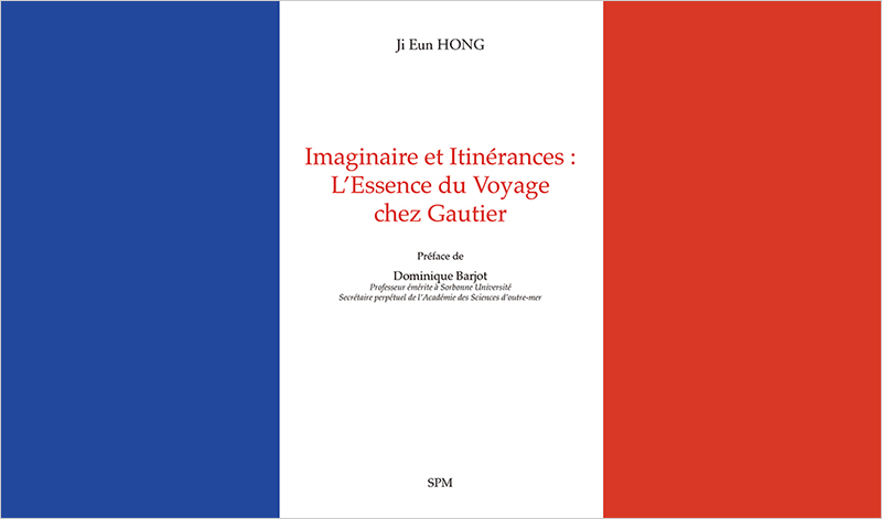
불어불문학과 홍지은(사진) 교수가 19세기 프랑스 작가 테오필 고티에(Théophile Gautier)의 작품 전반을 여행의 관점에서 재해석한 학술 저서 『Imaginaire et Itinérances : L'Essence du Voyage chez Gautier(상상과 여정: 고티에 문학에서 여행의 본질)』를 4월 28일 프랑스 SPM(Kronos) 출판사에서 출간했다.- 저서 출판 링크
SPM(Kronos)은 프랑스 나폴레옹 재단의 후원 아래 나폴레옹 관련 학술서를 독점 출판하며, 소르본 대학 교수진의 주요 저서를 펴내는 권위 있는 학술 출판사로 알려져 있다. 해당 도서는 지난 5월 프랑스 국립해외과학아카데미에서 영상으로도 소개됐다.

【홍지은 교수】
홍지은 교수의 신간은 19세기 프랑스 작가 테오필 고티에의 전 작품을 아우르며, 스페인에서 콘스탄티노플에 이르는 여행의 상상적 본질과 문학적 의미를 심층적으로 분석한 연구서다.
특히 고티에가 타문화를 공감과 상상의 언어로 이해하고자 했던 태도에 주목해, 문화적 다양성의 존중을 근간으로 하는 현대 공공외교의 정신과도 접점을 갖는다는 점을 강조한다. 문학적 상상력이 국경을 넘어 인문학적 대화의 토대가 될 수 있음을 보여주는 작업이기도 하다.
또한, 이 책에는 소르본 대학 명예교수이자 전 교육부 차관, 현 프랑스 국립해외과학아카데미(Académie des Sciences d'outre-mer) 종신회장인 도미니크 바르조(Dominique Barjot) 교수가 서문을 실어 출간의 의미를 더했다.
홍 교수의 저서는 최근 프랑스 국립해외과학아카데미 홈페이지(아래 링크)에 소개되기도 했다. 서평은 프랑스 리옹 3대학교 전 총장인 기 라롤(Guy Larole) 교수가 작성했다.
- https://www.academieoutremer.fr/presentation-bibliotheque-les-recensions-du-carasom/?aId=3691
홍지은 교수는 파리 소르본 대학에서 프랑스 문명 및 문학을 전공해 학사·석사·박사 학위를 취득했다. 미국 펜실베이니아대·존스홉킨스대, 독일 베를린 및 하이델베르크대 등 세계 유수 대학의 학술지에 단독 저자로 다수의 논문을 발표하며 국제 학계에서 활발히 활동하고 있다. 2020년에는 미국 로리안 헤밍웨이 단편소설 공모전 수상 등 문학 창작 분야에서도 성과를 거둔 바 있다.
한편, 홍지은 교수는 프랑스 국립 중앙은행 및 파리 소르본 대학 후원으로 6월 프랑스 경제사 학술지 『Revue française d'histoire économique』에 부산대 최재원 총장의 서문이 게재된 한국 특별판(N° 25, 2026-1)의 편집자로 초청되기도 했다.
※ 프랑스 국립 해외과학아카데미(Académie des sciences d’outre-mer, ASOM)
ASOM은 프랑스 고등교육·연구부 산하의 권위 있는 학술기관이자 공공행정기관으로, 1922년 창립 이후 유럽, 아프리카, 아시아, 라틴아메리카, 오세아니아를 잇는 국제 네트워크를 바탕으로 프랑코포니 세계의 학문·외교·문화 교류를 촉진해 오고 있다.
회원으로는 프랑스 대통령 3인과 총리 4인, 르클레르 드 오트클로크 원수, 모나코 알베르 2세를 비롯해 덴마크 왕실과 벨기에 국왕 등 유럽 왕실 인사들이 포함돼 있다. 또한 부트로스 부트로스-갈리 전 유엔 사무총장, 세네갈·포르투갈·브라질 등 각국의 전직 대통령들이 해외 회원으로 활동 중이다.
https://www.academieoutremer.fr
* 상단 이미지: 신간 표지.
Publication Details
Prof. Hong Ji-eun of the Department of French Language and Literature at Pusan National University (President: Choi Jae-won) has published Imaginaire et Itérances. L'Essence du Voyage chez Gautier (April 28) through French publisher SPM (Kronos) a prestigious academic house known for publishing Sorbonne faculty works and Napoleonic scholarship under the patronage of the Fondation Napoléon. Distribution is handled by L'Harmattan, and the book will be featured at ASOM in May.
The book features a preface by Prof. Dominique Barjot Sorbonne Professor Emeritus, former Vice-Minister of Education of France, and current Lifetime President of ASOM - lending considerable scholarly prestige to the publication.
About the Author
Prof. Hong earned her B.A., M.A., and Ph.D. in French Civilization and Literature from Paris Sorbonne University. She has published numerous solo-authored articles in academic journals affiliated with leading universities, including the University of Pennsylvania, Johns Hopkins University, and the Universities of Berlin and Heidelberg, and is a 2020 laureate of the Lorian Hemingway Short Story Competition. She has also been invited as editor of a special Korean edition (No. 25, 2026-1) of the French economic history journal Revue française d'histoire économique, supported by the Banque de France and Sorbonne University, featuring a preface by PNU President Choi Jae-won, due for publication in France in early June 2026.
- Author: HONG Ji Eun (Departement of French Langauge and Literature)
- Title of original paper: Imaginaire et Itinérances : L'Essence du Voyage chez Gautier
- Contact e-mail: cfje1003@gmail.com
-
지방세포 사멸이 염증성 면역세포 증가시켜 간에 지방 축적
제약학과/_UPLOAD/IMAGE/Board/68/2026/7/pLtQMjRXwQxSPSum.JPG제약학과황성환 교수팀 "비만이 부른 지방간…'죽은 지방세포'가 간질환 키운다"지방세포 사멸이 염증성 면역세포 증가시켜 간에 지방 축적
비만으로 인해 지방조직이 손상되면, 이 과정에서 죽은 지방세포가 간 건강까지 악화시킬 수 있다는 연구 결과가 나왔다.제약학과 황성환 교수팀은 비만으로 손상돼 죽은 지방세포가 염증성 면역세포인 S100A8 양성 대식세포를 간으로 끌어들여 지방 축적을 늘리고, 그 결과 대사이상 지방간질환(MASLD)을 악화시킨다는 분자 기전을 새롭게 밝혀냈다.
대사이상 지방간질환은 간에 지방이 과도하게 쌓이는 질환으로, 전 세계 성인 약 30%에서 나타나는 대표적인 대사질환이다. 비만이 주요 위험인자로 꼽혀 왔지만, 비만 상태에서 죽은 지방세포가 어떤 과정을 거쳐 간세포에 지방을 더 쌓이게 만드는지는 명확히 알려지지 않았다.
이번 연구에서는 비만 상태의 지방세포가 사멸하면서 유리지방산(FFA)과 세포외소포체(EV)를 방출하고, 이 신호가 간 안에 S100A8 양성 대식세포를 축적시킨다는 사실을 확인했다.
대식세포는 몸속에서 이물질을 제거하고 염증 반응을 조절하는 면역세포다. 이 가운데 S100A8 양성 대식세포는 염증 반응과 밀접한 S100A8 단백질을 많이 만드는 특정 대식세포 집단이다. 이 대식세포들이 간으로 이동하면, 원래 간세포의 지방 흡수를 억제하는 단백질인 CCN3의 발현이 줄어든다. CCN3는 세포 성장과 대사 조절에 관여하는 단백질로, 간세포 표면에서 지방산을 받아들이는 통로 역할을 하는 CD36의 발현을 억제하는 기능이 있다.
하지만 S100A8 양성 대식세포가 늘어나면 CCN3가 감소하고, 그 결과 CD36 발현이 증가해 간세포가 지방산을 더 많이 흡수하게 된다. 결국 간 안에 지방이 과도하게 축적되면서 지방간질환이 더 심해지는 것이다.
연구팀은 이런 과정을 규명하기 위해 독창적인 유전자 변형 동물모델을 활용했다. 대식세포에서만 S100A8 유전자가 없도록 만든 마우스와 지방세포가 죽지 않도록 항세포사멸 유전자 BCL2를 과발현시킨 마우스를 구축해 지방세포 사멸과 간 염증, 지방 축적의 연관성을 추적했다.
또 단일세포 전사체 분석(scRNA-Seq)을 통해 지방세포 사멸 신호가 간 내 S100A8 양성 대식세포를 증가시킨다는 점도 확인했다. 단일세포 전사체 분석은 세포 하나하나의 유전자 발현 상태를 정밀하게 분석해 어떤 세포가 늘고 줄었는지, 어떤 기능을 하는지 파악하는 기술이다.

【S100A8 양성 대식세포에 의한 간세포의 지방축적 기전】
연구의 핵심은 지방간질환을 간 자체의 문제만으로 보지 않고, 지방조직과 간 사이의 상호작용이라는 관점에서 풀어냈다는 데 있다. 연구팀은 지방세포 사멸 → 간의 S100A8 양성 대식세포 증가 → CCN3 감소 → CD36 증가 → 간세포 지방 축적이라는 연쇄 경로를 제시하며, 비만이 지방간을 악화시키는 새로운 장기 간 상호작용 기전을 설명했다.
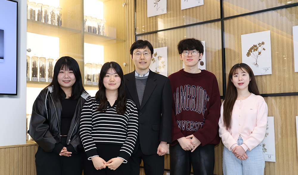
이번 연구는 미국 국립보건원(NIH) 산하 국립 알코올남용·알코올중독연구소(NIAAA) Bin Gao 박사 연구팀과의 국제 공동연구로 진행됐다. NIAAA 측이 동물모델 구축을, 부산대 연구팀이 분자 기전 분석을 맡아 융합 연구 성과를 냈다. 과학기술정보통신부 우수신진연구사업 지원을 받았으며, 제약학과 황성환 교수가 교신저자, 김연수 석박사통합과정생이 제1저자로 수행했다.
해당 연구 결과는 국제학술지 『Journal of Clinical Investigation』 2025년 11월 3일자에 게재됐다.
- 논문 제목: Adipocyte death promotes hepatic infiltration of S100A8+ macrophages and steatotic liver disease progression in mice (지방세포 사멸이 마우스에서 S100A8 양성 대식세포의 간 내 침윤과 지방간질환의 진행을 촉진한다)
- 논문 링크: https://www.jci.org/articles/view/190635
황성환 교수는 “이번 연구는 지방간질환의 원인을 간 자체가 아닌, 비만으로 손상된 지방조직과 간 사이의 상호작용에서 규명했다는 점에서 의미가 크다”며 “S100A8 양성 대식세포의 병인적 역할을 제시한 중요한 성과”라고 말했다.
연구팀은 이번 성과가 향후 지방세포 사멸, S100A8 양성 대식세포, CD36 매개 지방 흡수 경로를 겨냥한 새로운 지방간질환 치료제 개발에 중요한 단서를 제공할 것으로 기대하고 있다.
* 상단 사진: 연구팀. 왼쪽부터 김연수 석박사통합과정생, 박윤서 석박사통합과정생, 황성환 교수, 정준영 석사과정생, 조예은 석박사통합과정생.
[Abstract]
Both adipocytes and hepatocytes have the capacity to store fat, but the factor(s) that determine fat distribution between these cell types remain unknown. In mice fed a high-fat diet, fat initially accumulates predominantly in adipocytes, while hepatic fat accumulation mainly emerges after the onset of epididymal adipocyte death that results in elevated free fatty acids to promote lipid accumulation in hepatocytes. However, it remains unclear whether other signals after adipocyte death are required to direct and/or promote hepatocytes to store fat and subsequently trigger metabolic dysfunction-associated steatotic liver disease (MASLD, formerly known as nonalcoholic fatty liver disease). Using genetically modified mouse models combined with bulk and single-cell RNA-Seq analysis, we demonstrated that visceral adipocyte death induced an accumulation of S100A8+ macrophages in the liver, which was partially induced by fatty acids and apoptotic adipocyte-derived extracellular vesicles. Macrophage-specific deletion of the S100a8 gene reduced hepatic fat accumulation and MASLD severity in mice. Mechanistically, S100A8+ macrophages suppressed cellular communication network factor 3 (CCN3), a negative regulator of CD36, thereby enhancing CD36 expression in hepatocytes. In conclusion, adipocyte death promotes hepatic infiltration of S100A8+ macrophages, which drive hepatocyte lipid storage and subsequently promote MASLD progression through CD36 upregulation, partially mediated by CCN3 suppression.
- Authors (Pusan National University)
· First author: Yeonsoo Kim (College of Pharmacy)
· Corresponding author: Seonghwan Hwang (College of Pharmacy)
- Title of original paper: Adipocyte death promotes hepatic infiltration of S100A8+ macrophages and steatotic liver disease progression in mice
- Journal: Journal of Clinical Investigation
- Web link: https://www.jci.org/articles/view/190635
- Contact e-mail: shhwang@pusan.ac.kr
-
트랜스젠더 사례 3만 건 분석, 우산형 문헌고찰 논문 발표
양산부산대병원/의과대학]/_UPLOAD/IMAGE/Board/68/2026/6/GoMlKUzrhb8L3zWw.JPG양산부산대병원/의과대학]김기훈 전임의·김윤학 교수팀 "성확정 호르몬 치료, 심혈관 위험 높지 않아"트랜스젠더 사례 3만 건 분석, 우산형 문헌고찰 논문 발표
양산부산대병원과 의과대학 공동 연구진이 성확정 호르몬 치료(Gender-Affirming Hormone Therapy, GAHT)의 심혈관 안전성을 세계 최초로 우산형 문헌고찰(umbrella review)*로 종합 평가해, 치료와 관련된 불확실성을 과학적으로 정리하고 임상 현장에서 활용 가능한 근거를 제시함으로써 환자 맞춤형 관리와 임상 가이드라인 및 보건 정책 수립에 도움을 줄 전망이다.* 우산형 문헌고찰(umbrella review): 기존에 발표된 체계적 문헌고찰(systematic review)과 메타분석(meta-analysis)을 다시 종합·평가하는 최상위 단계의 문헌고찰 방법.
양산부산대병원 직업환경의학과 김기훈 전임의와 의과대학 융합의과학과 김윤학 교수 연구팀은 성확정 호르몬 치료의 심혈관 안전성을 종합적으로 규명한 연구 논문을 국제 학술지 『International Journal of Transgender Health』 1월 1일자에 게재했다.
- 논문 제목: Gender-affirming hormone therapy and cardiovascular risk: an umbrella review of meta-analyses (성확정 호르몬 치료와 심혈관 위험: 메타분석을 대상으로 한 우산형 문헌고찰)
- 논문 링크: https://doi.org/10.1080/26895269.2025.2608831
이번 연구는 기존에 발표된 개별 메타분석 연구들을 통합·재평가한 ‘우산형 문헌고찰’ 연구로, 성확정 호르몬 치료를 시행받은 트랜스젠더 인구 3만 명 이상을 포함한 8편의 메타분석 연구를 체계적으로 분석했다.
연구팀은 PRISMA* 가이드라인을 준수해 문헌을 선별했으며, AMSTAR-2**와 GRADE*** 평가 체계를 적용해 근거의 질과 신뢰도를 엄격히 평가했다. 이를 통해 성확정 호르몬 치료가 심혈관 건강 및 주요 심혈관 사건에 미치는 영향을 종합적으로 분석했다.
* PRISMA: Preferred Reporting Items for Systematic Reviews and Meta-Analyses. 체계적 문헌고찰과 메타분석 논문을 투명하고 일관되게 보고하기 위한 국제 표준 보고 지침.
** AMSTAR-2: 체계적 문헌고찰·메타분석의 방법론적 질과 신뢰도를 평가하는 도구.
*** GRADE: 종합된 연구 결과(body of evidence)에 대한 근거의 확실성(신뢰 수준)을 평가하는 체계.
연구 결과, 출생 시 여성으로 지정된(AFAB) 대상자에서 테스토스테론 치료 후 LDL 콜레스테롤과 중성지방 증가, HDL 감소 등 지질대사 변화가 관찰됐으나, 정맥혈전색전증(VTE), 심근경색, 뇌졸중 등 주요 심혈관 사건 발생 위험이 유의하게 증가한다는 근거는 제한적인 것으로 나타났다. 출생 시 남성으로 지정된(AMAB) 대상자에서는 전반적인 심혈관 지표 변화가 상대적으로 크지 않았다.

【성확정 호르몬 치료(GAHT)의 심혈관 안전성에 대한 우산형 문헌고찰 개요 모식도】
이번 연구의 개요, 주요 결과 및 임상적 의의를 요약한 모식도로,
출생 시 여성으로 지정된(AFAB) 대상자에서는 지질대사 지표(LDL, 중성지방 등)의 일부 변화가 관찰된 반면,
정맥혈전색전증, 심근경색, 뇌졸중 등 주요 심혈관 사건의 위험이 유의하게 증가한다는 근거는 제한적임을 보여준다.
연구팀은 “성확정 호르몬 치료(GAHT)가 대사 지표에는 영향을 미칠 수 있으나, 현재까지의 근거로는 단·중기적으로 심혈관 사건 위험이 뚜렷하게 증가한다고 단정하기 어렵다”고 설명하며, 개별 환자의 심혈관 위험요인을 고려한 맞춤형 모니터링의 중요성을 강조했다.
이번 연구는 성확정 호르몬 치료의 심혈관 안전성에 대한 최상위 근거를 제시해 임상적 불확실성을 줄이고, 환자 맞춤형 위험 평가·관리와 향후 임상 가이드라인 수립 등에 활용될 수 있을 것으로 기대된다.
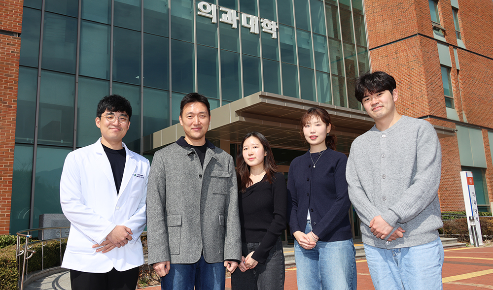
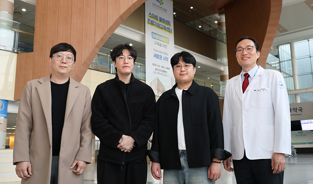
이번 연구에 참여한 의료기관은 △연세대 의과대학 △과학기술연합대학원대 △한국과학기술연구원 △가천대 길병원 △부산대 △부산대병원 △양산부산대병원 △부산대치과병원 등 총 8곳이며, 부산대 의과대학 문현오 박사과정생, 박세진 박사과정생, 이영인 학생이 공동 제1저자, 한국과학기술연구원(KIST) 김원규 교수, 양산부산대병원 김기훈 전임의, 부산대 의과대학 김윤학 교수가 공동 교신저자로 수행했다.
이번 연구는 과학기술정보통신부·교육부 재원으로 수행된 한국연구재단 연구사업, 보건복지부 재원의 한국보건산업진흥원(KHIDI)을 통한 보건의료기술연구개발사업, 산업통상자원부 재원의 한국산업기술진흥원(KIAT)을 통한 산업혁신인력개발사업, 식품의약품안전처 재원의 연구개발사업 등의 지원을 받아 수행됐다.
* 연구진 사진: 왼쪽부터 양산부산대병원 김기훈 전임의, 의과대학 김윤학 교수, 이영인·박세진·문현오 학생.
[Abstract]
Introduction: Gender-affirming hormone therapy (GAHT) is widely used to help transgender individuals align physical traits with gender identity, yet concerns remain regarding its cardiovascular safety. Previous reviews have produced conflicting findings, often constrained by small sample sizes, short follow-up, and heterogeneous hormone regimens. This umbrella review synthesizes current meta-analytic evidence on cardiovascular outcomes of GAHT.
Methods: We followed PRISMA guidelines and searched Embase, MEDLINE, Scopus, Web of Science, and ScienceDirect through February 2025. Eligible studies were meta-analyses reporting quantitative outcomes of GAHT. Data were extracted on lipid profiles, blood pressure, hematocrit, and cardiovascular events. Pooled estimates were calculated using inverse-variance methods. Study quality was assessed with AMSTAR 2, and evidence certainty was graded with GRADE.
Results: Eight meta-analyses including 30,789 participants were reviewed. Among individuals assigned female at birth (AFAB), GAHT increased low-density lipoprotein, triglycerides, and total cholesterol and decreased high-density lipoprotein. Blood pressure showed no significant change. Among individuals assigned male at birth (AMAB) receiving estradiol, lipid effects were inconsistent. Hematocrit increased predominantly in the AFAB group. VTE prevalence was 0.01 in AFAB and 0.02 in AMAB, while risks of myocardial infarction and stroke were not significantly different. The overall quality of evidence ranged from moderate to low.Conclusions: GAHT affects lipid metabolism, especially among AFAB individuals, but current data do not indicate a significant increase in cardiovascular events. Given the short follow-up and heterogeneity of study designs, further high-quality research is warranted to guide clinical care.
- Authors (Pusan National University)
· Hyunoh Moon, Sejin Park, Yeongin Lee (School of Medicine)
· Kihun Kim (Department of Occupational and Environmental Medicine)
· Yun Hak Kim (Department of Anatomy and Biomedical Informatics)
- Title of original paper: Gender-Affirming Hormone Therapy and Cardiovascular Risk: An Umbrella Review of Meta-Analyses
- Journal: International Journal of Transgender Health
- Web link: https://www.tandfonline.com/doi/full/10.1080/26895269.2025.2608831
- Contact e-mail: kihun7603@punyh.co.kr / yunhak10510@pusan.ac.kr
-
단계별 최소 강도 수학적으로 규명…맞춤형 아토피 치료 기대
G-램프사업단/_UPLOAD/IMAGE/Board/68/2026/6/sh06C0AK2jEdpkls.JPGG-램프사업단강요셉 연구원팀, 중증 아토피 피부염 치료 강도 예측 모델 개발단계별 최소 강도 수학적으로 규명…맞춤형 아토피 치료 기대
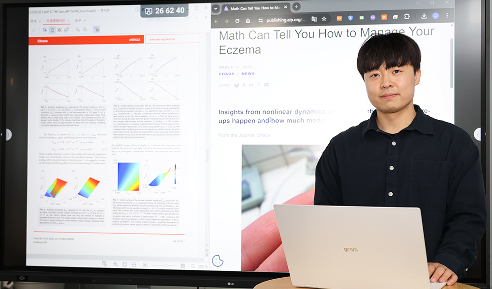
G-램프(LAMP)사업단 미래지구환경연구소 강요셉(사진) 연수연구원 국제공동연구팀이 아토피 피부염의 단계별 치료에 필요한 ‘최소 약물 강도’를 수학적으로 규명해, 환자 상태 기반의 정량적 치료 전략 수립 가능성을 제시했다.강요셉 연구원은 미국 애리조나주립대와의 공동연구를 통해 중증 아토피 피부염의 치료 과정을 비선형 동역학 시스템*으로 모델링하고, 임상에서 흔히 쓰이는 2단계(초기-유지) 치료 전략을 수학적으로 제시했다.
* 비선형 동역학 시스템(non-linear dynamical system): 시간에 따라 변하는 어떤 상태(state)를 식으로 모델링할 때, 그 변화 규칙이 ‘선형’이 아닌 시스템.
아토피 피부염은 만성 염증성 질환으로 재발이 잦고 장기 치료가 필요한 대표적인 난치성 질환이다. 특히 중증 아토피 피부염의 경우 치료 반응이 제한적이며, 환자별 상태에 따라 얼마나 강한 치료가 필요한지에 대한 정량적 기준이 부족해 경험적 판단에 의존하는 한계가 있었다.
이에, 연구팀은 아토피 피부염을 비선형 동역학 시스템으로 모델링하고, 치료 과정을 급성 염증을 억제하기 위해 항생제를 투여하는 ‘초기 치료 단계(Get Control)’와 증상이 가라앉은 상태(remission)를 유지하기 위해 보습제를 적용하는 ‘유지 단계(Keep Control)’의 2단계로 나눠 치료 전략에 대한 수학적 틀을 확립했다. 연구팀이 치료적으로 가장 중요하게 던진 질문은 ‘각 단계가 성공하기 위해 필요한 최소 약물 용량은 얼마인가?’였다.
분석 결과, 제어의 크기(약물 용량)는 중증 아토피 피부염을 결정짓는 두 가지 근본 요인, 즉 피부 장벽의 투과성(barrier permeability)과 면역 제거 능력(immune clearance capacity)에 직접적으로 연결돼 있었다. 연구팀은 초기 치료 단계에서 만성 염증 상태를 벗어나기 위해 필요한 항생제 용량과 유지 단계에서 증상이 가라앉은 상태를 지속하기 위해 필요한 보습제 수준을 구체적으로 구분해 제시했다.

【중증 아토피피부염의 2단계 제어 전략 개념도(Get Control–Keep Control)】
상단은 시간에 따른 아토피피부염(AD) 중증도의 변화를, 하단은 피부 장벽 상태의 회복 과정을 나타낸다.
초기의 Get Control (GC) 단계에서는 단기간의 집중 치료를 통해 질병 중증도를 빠르게 감소시키며,
이후 Keep Control (KC) 단계에서는 유지 치료를 통해 안정적인 상태를 지속한다.우선, 초기 치료 단계에서는 항생제 최소 강도가 피부 장벽 상태와 면역 반응에 따라 선형 또는 구간별 선형 관계를 따르는 것으로 나타났다. 즉 피부 장벽이 더 손상됐거나 면역 제거 능력이 낮을수록 만성 염증 상태를 벗어나기 위해 더 강한 초기 개입이 필요하며, 반대로 상태가 비교적 양호하면 낮은 강도 치료로도 염증 억제가 가능할 수 있음을 시사한다.
반면 유지 단계에서는 보습제 요구량이 비선형적으로 증가하며, 피부 장벽이 약할수록 급격히 증가하는 특성이 확인됐다. 이는 중증 아토피 관리에서 염증을 가라앉히는 것만으로는 부족하며, 장벽의 구조적 취약성을 안정화하는 장기 유지 전략이 치료 성패를 좌우한다는 점을 강조한다.
연구팀은 이번 성과가 중증 아토피 치료를 ‘경험적 판단’에서 ‘정량적 제어’ 문제로 재구성했다는 점에서 학술적·임상적 의미가 크다고 설명했다. 또한 피부 장벽 손상, 미생물 변화, 면역 이상 등 복합 요인을 시간에 따라 변하는 동역학 시스템으로 연결해 병태 메커니즘과 수학 모델을 결합한 융합 연구 사례로 소개했다.
향후 환자별 장벽 지표, 염증 정도, 재발 패턴 등 실제 임상 데이터를 이 모델에 결합하면, 개인별 최적 초기 치료 강도와 유지 치료 수준을 더 정밀하게 예측해 최소한의 약물로 치료 효과를 극대화 할 수 있는 전략 수립에 기여할 것으로 기대된다.

【아토피피부염 병태생리 과정의 개념적 모식도와 동역학적 상태 분류】
(a)는 치료가 없는 경우와 치료가 적용된 경우를 모두 포함하는 아토피피부염(AD) 병태생리의 핵심 수학 모델을 도식화한 것이다.
환경적 자극은 병원체(P)를 증가시키고 선천면역반응(R)을 활성화하며, 이는 칼리크레인(K) 발현을 유도해 피부 장벽(B)을 손상시킨다.
장벽 손상은 병원체 침투를 더욱 촉진해 염증을 지속시키며, 수지상세포(D)의 축적은 Gata3(G)를 활성화시켜 만성 상태를 유도한다.
항생제(A)는 병원체를 직접 억제하고, 보습제(E)는 피부 장벽 회복을 촉진한다.이번 연구는 교육부·한국연구재단의 중점테마연구소(G-LMAP)지원사업을 통해 강요셉 연구원이 교신 및 제1저자로 수행했다. 해당 논문은 ‘Controlling severe atopic dermatitis dynamics(중증 아토피 피부염 동역학의 제어)’라는 제목으로 국제 학술지 『Chaos』 3월 17일자 Featured Article로 소개됐다.
- 논문 링크: https://doi.org/10.1063/5.0308283
강요셉 연구원은 “이번 연구는 ‘얼마나 치료해야 하는가’라는 임상적 질문에 대해 수학적으로 답을 제시한 데 의미가 있다”며 “환자 상태에 맞는 최적의 치료 강도를 설계할 수 있는 기반을 마련했다”고 말했다.
[Abstract]
Atopic dermatitis (AD) is a pervasive inflammatory skin disease, with severe forms constituting a refractory phenotype that devastates quality of life through relentless pruritus, widespread lesions, and resistance to standard therapies. A central clinical challenge is to steer the disease away from chronic inflammation and sustain remission. Framed in dynamical terms, this amounts to controlling the remission dynamics of AD. We establish a mathematical x-x-framework for the canonical two-phase clinical strategy: the “Get Control” (GC) phase, where antibiotics are administered to suppress acute inflammation, and the “Keep Control” (KC) phase, where emollients are applied to maintain remission. A key question of therapeutic relevance is: what are the minimal drug doses required for each phase to succeed? Our analysis reveals scaling laws that tie the control amplitude (drug dose) directly to two fundamental determinants of severe AD: barrier permeability and immune clearance capacity. These laws delineate the antibiotic dosage required to exit chronic inflammation in GC and the emollient level needed to sustain remission in KC. The uncovered scaling principles elevate treatment design from heuristic to quantitative, leading to a theoretical x-x-framework for precision, phase-based analysis of treatment control in severe AD. By aligning clinical intervention with the dynamical structure of the disease, the x-x-framework points toward personalized, optimally dosed strategies for overcoming refractory cases.
- Author (Pusan National University): Yoseb Kang (Mathematics Department)
- Title of original paper: Controlling severe atopic dermatitis dynamics
- Journal: Chaos
- Web link: https://doi.org/10.1063/5.0308283
- Contact e-mail: josephdytpq@pusan.ac.kr
-
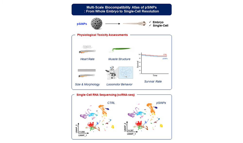
개체부터 세포까지 멀티스케일 평가…세포 유형별 스트레스·면역·대사 반응 정밀 규명
융합의과학과/_UPLOAD/IMAGE/Board/68/2026/5/oVuXV8XTLt2mwnLO.JPG융합의과학과오창규 교수팀, 제브라피시·단일세포 분석으로 다공성 실리콘 나노입자 '생체적합성 지도' 구축개체부터 세포까지 멀티스케일 평가…세포 유형별 스트레스·면역·대사 반응 정밀 규명
나노소재 기반 약물전달 기술이 항암 치료와 정밀의학의 핵심 플랫폼으로 떠오르고 있지만, 실제 생체 내에서 어떤 조직/어떤 세포가 어떻게 반응하는지까지 정밀하게 확인할 수 있는 안전성 평가 체계는 아직 충분하지 않다. 기존 독성 평가는 주로 생존율, 형태 이상, 조직 손상 등 개체(whole organism) 또는 조직 수준 지표에 의존해 왔기 때문에, 나노입자 특성에 따라 달라질 수 있는 세포 유형별 반응과 분자 수준 변화를 놓치기 쉽다는 한계가 있었다.이에, 융합의과학과 오창규 교수와 김윤학 교수 연구팀은 다공성 실리콘 나노입자(porous silicon nanoparticles, pSiNPs)의 생체적합성을 개체에서 단일세포 해상도까지 한 번에 연결해 분석하는 다중 스케일(multi-scale) 전략을 제시해 관심을 모으고 있다. 연구팀은 투명하고 발달이 빠르며 독성·발생 연구에 널리 활용되는 제브라피시 배아(zebrafish embryo) 모델을 이용해 pSiNPs 노출 후 생존율, 형태학적 변화, 장기 발달, 심박수 등 거시적 지표를 먼저 평가했다. 이어 동일 조건에서 확보한 시료를 대상으로 단일세포 RNA 시퀀싱(scRNA-seq)을 수행해, 개별 세포 단위에서 유전자 발현 변화를 정밀하게 추적했다.
특히 이번 연구의 핵심은 개체 수준에서 관찰되는 표현형(phenotype)과 단일세포 전사체 변화(transcriptomic response)를 유기적으로 연결해, 조직 및 세포 유형별 반응을 한눈에 볼 수 있는 고해상도 ‘생체적합성 지도(biocompatibility atlas)’를 구축했다는 점이다.
분석 결과, pSiNPs는 전반적으로 높은 생체적합성을 보였으며, 단일세포 수준에서도 세포 구성 및 유전자 발현 변화가 거의 관찰되지 않았다. 특히 산화 스트레스, 면역 반응, 세포 사멸 등 독성과 관련된 주요 경로에서도 유의한 변화가 확인되지 않아, 세포 유형 전반에 걸쳐 안정적인 생체 반응을 나타냈다.

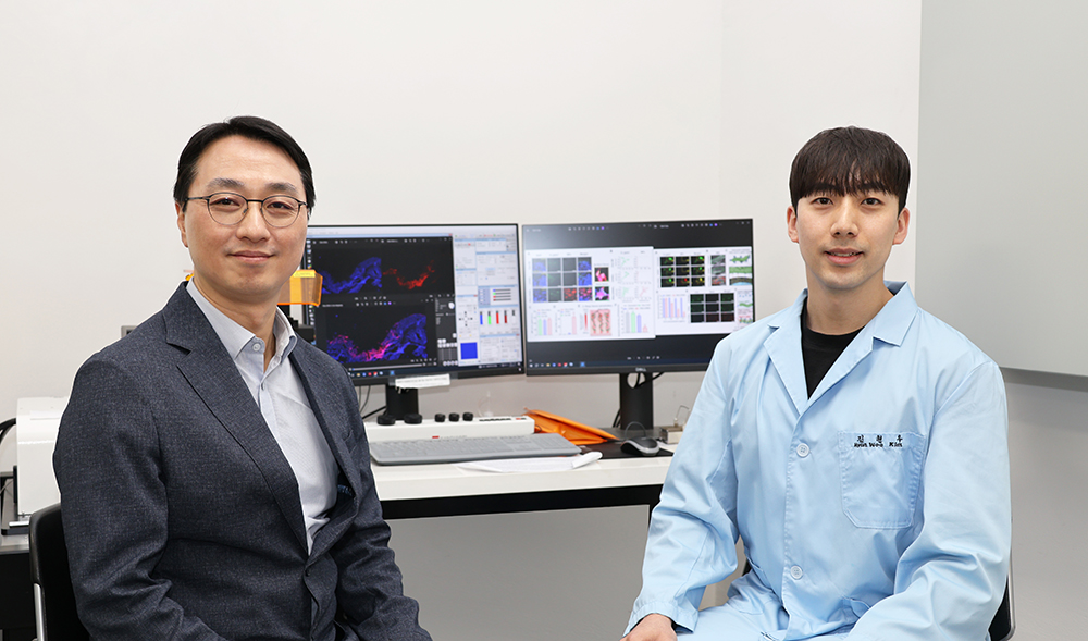
【연구진 왼쪽부터 오창규 교수, 권은정 박사후연구원, 김예진 박사과정생】연구팀은 이번 플랫폼이 특정 소재(pSiNPs)에만 국한되지 않고, 향후 다양한 나노소재에도 적용 가능한 체계적 생체적합성 스크리닝 프레임워크가 될 수 있다고 강조했다. 개체 수준 독성 결과와 단일세포 전사체 데이터를 통합해 해석함으로써, 나노소재 기반 치료제 개발 과정에서 안전성 평가의 기준을 고도화하고, 세포 유형별 반응 메커니즘을 바탕으로 한 정밀한 설계·개선 전략 수립에도 기여할 것으로 기대된다.
이번 연구는 경희대와의 공동연구로 수행됐으며, 융합의학과 오창규 교수와 의학과 및 융합의과학과 김윤학 교수가 공동 교신저자, 의학연구원 소속 권은정 박사후연구원, 융합의과학과 김예진 박사과정생이 공동 제1저자로 참여했다. 국제 학술지 『Biomaterials』 온라인 3월 12일자에 소개됐으며, 8월호에 게재될 예정이다.
- 논문 제목: A Multi-Scale Biocompatibility Atlas of Porous Silicon Nanoparticles: From Whole Embryo to Single-Cell Resolution(다공성 실리콘 나노입자의 생체 적합성 아틀라스: 개체 수준에서 단일 세포 해상도까지의 통합적 분석)
- 논문 링크: https://pubmed.ncbi.nlm.nih.gov/41833253
* 상단 연구 이미지: pSiNP의 다중 스케일 생체 적합성 지도: 전체 배아에서 단일 세포 해상도까지
[Abstract]
The clinical translation of nanomedicines, such as porous silicon nanoparticles (pSiNPs), requires rigorous and multidimensional safety evaluation that extends beyond conventional in vitro assays, which often fail to capture complex in vivo interactions. Here, we establish a multi-scale assessment pipeline employing the zebrafish (Danio rerio) model, integrating whole-organism phenotyping with single-cell RNA sequencing (scRNA-seq) for high-resolution biological profiling. Zebrafish embryos demonstrated exceptional tolerance to pSiNPs, with no observable changes in survival, developmental morphology, or overall growth. Transient and mild reductions in cardiac and locomotor activity observed 2 h post-exposure were fully restored within 24 h, indicating minimal physiological perturbation. At the molecular level, unbiased scRNA-seq analyses revealed a largely quiescent transcriptomic landscape: pSiNP exposure did not disrupt cellular composition or activate gene programs related to stress, toxicity, or inflammation. This integrative, organism-to-single-cell blueprint of biocompatibility provides compelling evidence supporting the safety of pSiNPs and highlights their potential as a robust platform for next-generation drug delivery and theranostic applications.
- Authors (Pusan National University)
∙ First authors: Eun Jung Kwon (Medical Research Institute), Yejin Kim (Department of Convergence Medical Sciences, School of Medicine)
∙ Corresponding authors: Yun Hak Kim (Department of Anatomy, School of Medicine), Chang-Kyu Oh (Department of Biochemistry, School of Medicine)
- Title of original paper: A Multi-Scale Biocompatibility Atlas of Porous Silicon Nanoparticles: From Whole Embryo to Single-Cell Resolution
- Journal: Biomaterials
- Web link: https://pubmed.ncbi.nlm.nih.gov/41833253
- Contact e-mail: Chang-Kyu Oh (ck1988@gmail.com)
-
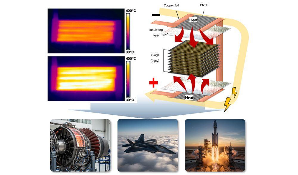
탄소나노튜브 필름 줄가열 공정 개발
응용화학공학부/_UPLOAD/IMAGE/Board/68/2026/5/QEInNEI6X1yqCgJC.JPG응용화학공학부성동기 교수팀 "기존 에너지의 5%만 쓰고도 항공우주 소재 만든다"탄소나노튜브 필름 줄가열 공정 개발
응용화학공학부 성동기 교수 연구팀이 항공우주 부품에 요구되는 경량화와 고내열성, 제빙 및 전자파 차폐(遮蔽) 성능을 동시에 갖춘 탄소섬유 복합재료를 높은 에너지 효율로 제조하는 기술을 개발했다. 이 기술을 적용하면 기존 대비 단 5% 수준의 에너지로도 가볍고 튼튼한 소재를 만들 수 있어, 항공우주를 비롯한 다양한 첨단 산업의 혁신이 기대된다.연구팀은 탄소나노튜브(CNT) 필름을 이용한 줄가열 공정을 개발해, 기존의 고분자 재료가 가진 내열성의 한계를 극복해 고온에서 안정할 뿐 아니라 항공우주 부품에 필수적인 제빙과 전자파 차폐 성능까지 갖춘 항공우주용 경량 탄소섬유 복합재료를 친환경적으로 제조할 수 있는 기술을 확보했다.
섬유강화 복합재는 가볍고 강도가 우수해 항공기, 우주 구조물, 자동차 등 다양한 산업 분야에서 널리 활용되고 있다. 특히 탄소섬유 복합재는 강철보다 가벼우면서도 높은 비강도(比强度)와 강성을 가져 차세대 항공우주 산업의 핵심 소재로 주목받고 있다.
최근 항공우주 분야에서는 엔진 구조물, 고온 환경에 노출되는 외장재 등 고온에서도 기계적 성능과 구조적 안정성을 유지할 수 있는 복합재에 대한 요구가 증가하고 있다. 그러나, 이를 위해서는 내열성이 우수한 폴리이미드 등 고내열 수지를 사용한 300℃ 이상의 고온 공정이 필요해 에너지 소모가 크고 높은 점도로 인해 고품질의 복합재 제작이 어렵다는 한계가 있다.
연구팀은 이 문제를 해결하기 위해, 기존처럼 금형 외부를 전체 가열하는 방식 대신 탄소나노튜브 필름을 탄소섬유에 배치해 전류를 흘려 직접 발열시키는 줄가열 공정을 제안했다.
이 기술은 전기에너지를 열에너지로 변환해 필요한 부위에 열을 직접 전달함으로써, 고온 프레스 장비를 쓰는 기존 공정 대비 약 5% 수준의 에너지만으로도 제조가 가능하고, 수지 함침성(含浸性)을 크게 높여 내부 기공을 효과적으로 억제했다. 그 결과 기계적 강도와 구조적 신뢰성이 향상됐으며, 유리전이온도 약 362 ℃ 수준의 고내열 특성을 확보해 고온 환경에서도 안정적인 성능을 유지할 수 있음을 확인했다.
또한, 탄소나노튜브 필름 도입으로 항공기 구조물에 필요한 제빙 및 전자파 차폐 성능을 동시에 확보했다. 특히, 성형 공정 중 탄소나노튜브 필름의 균일한 발열 특성은 복합재 두께 방향의 온도 편차를 최소화해 구조적 안정성을 향상시켰으며, 대면적 구조물로의 확장이 가능한 에너지 효율적 공정임을 검증했다.
이번에 개발한 복합재 제조 기술은 항공기 외장재, 엔진 구조물 등 300℃ 이상의 고내열·다기능 특성이 요구되는 항공 우주 분야를 비롯해 에너지 효율적 대면적 구조물 제조가 필요한 다양한 첨단 산업 분야로의 확장이 기대된다.
성동기 교수는 “탄소섬유 복합재료는 높은 강도를 가진 경량소재로서 다양한 산업에 적용되고 있지만, 내열성이 낮아서 고온 환경에서의 적용성은 제한적이다. 이번 연구에서는 탄소나노튜브 필름을 활용한 새로운 줄가열 공정을 통해 고내열 탄소섬유 복합재료를 기존 기술 대비 낮은 에너지로 제조하는 공정 기술을 제안했다. 특히 유리전이온도 362 ℃ 수준의 고온 안정성과 제빙·전자파 차폐 기능을 하나의 구조 내에 통합함으로써, 항공기 외장재와 우주 구조체 등 극한 환경용 차세대 구조물에 적용 가능한 핵심 기술로 발전할 수 있을 것으로 기대된다”고 말했다.

【연구진: 왼쪽부터 성동기 교수, 정미주 석사 졸업생, 김송희 석사과정생, 김다영 석박사통합과정생】
이번 연구는 부산대 응용화학공학부 성동기 교수가 교신저자, 정미주 석사 졸업생, 김송희 석사과정생, 김다영 석박사통합과정생이 공동 제1저자로 수행했으며, 한국재료연구원과 미국 텍사스주립대(The University of Texas at Austin)가 공동연구로 참여했다.
해당 연구 성과는 학술지 국제 학술지 『Composites Part B: Engineering』 4월호에 게재됐다.
- 논문 제목: CNT film-integrated polyimide composites: Scalable joule heated infusion process and multifunctional aerospace applications(탄소나노튜브필름이 통합된 폴리이미드 복합재료: 확장 가능한 줄 가열 공정 및 다기능 항공우주 응용)
- 논문 링크: https://doi.org/10.1016/j.compositesb.2026.113471
이번 연구는 과학기술정보통신부와 한국연구재단이 추진하는 나노소재기술개발사업 및 미래기술연구실 지원을 받았다.
※ 용어 설명
- 탄소섬유: 탄소 함량이 매우 높은 가볍고 강한 섬유로서 고강도·고탄성 특성이 필요한 항공우주, 자동차, 스포츠용품 등에 널리 사용됨.
- 탄소나노튜브 필름: 탄소나노튜브를 얇은 필름 형태로 집적한 전도성 소재로, 우수한 전기·열 전도성과 경량 특성을 동시에 가져 다양한 기능성 응용 분야에 활용됨.
- 줄가열 공정: 전도성 물질에 전기를 가하면 열이 발생하는 원리를 이용하여 고분자 재료를 녹이고 경화하는 공정으로 비싼 장비없이 낮은 전기에너지로 복합재료 생산이 가능함.
* 상단 연구 이미지: CNT 필름 기반 줄가열 공정을 이용한 탄소섬유 복합재료 제조공정 및 항공우주 응용. CNT 필름을 줄가열 장치로 활용해 높은 에너지 효율로 폴리이미드를 녹이고 경화함으로써 고내열 탄소섬유 복합재료를 제조하는 공정 기술(위)과 이를 이용해 다양한 항공우주 산업에 적용할 수 있는 응용 분야(아래)를 나타냄.
[Abstract]
Researchers at Pusan National University have developed a carbon nanotube (CNT) film based Joule heating infusion process for manufacturing high-temperature carbon fiber-reinforced polyimide composites for aerospace applications. By directly converting electrical energy into heat through CNT films, the process enables uniform thermal delivery, significantly reducing void formation and improving mechanical reliability. The resulting composite achieved a glass transition temperature of approximately 362 ℃ while requiring only about 5% of the energy consumption of conventional hot pressing. Furthermore, the integrated CNT film provides additional multifunctional properties, including de-icing capability and enhanced electromagnetic interference shielding. This study presents an energy-efficient and scalable manufacturing platform for high-performance, multifunctional aerospace composites.
- Authors (Pusan National University)
· Co-first authors: Mi Ju Jeong, Song Hee Kim, Dayoung Kim (School of Chemical Engineering)
· Corresponding author: Dong Gi Seong (Department of Polymer Science and Engineering / School of Chemical Engineering)
- Title of original paper: CNT film-integrated polyimide composites: Scalable joule heated infusion process and multifunctional aerospace applications
- Journal: Composites Part B: Engineering
- Web link: https://doi.org/10.1016/j.compositesb.2026.113471
- Contact e-mail: dgseong@pusan.ac.kr
-
내비게이션 기관지내시경 정밀도 향상 AI 모델 개발
의생명융합공학부·양산부산대병원/_UPLOAD/IMAGE/Board/68/2026/4/7jKaAQGmwuSanBpb.JPG의생명융합공학부·양산부산대병원김민우·설희윤 교수팀, CT에서 누락된 말초 기도까지 AI로 찾아낸다내비게이션 기관지내시경 정밀도 향상 AI 모델 개발
기관지 CT 영상에서 전문가(의사/연구자)가 ‘이 부분이 기도(airway)’임을 표시해 둔 ‘주석’이 없는 부분은 대개 배경으로 인식돼 기도의 말초 가지를 놓치기 쉽다. 이에 주석이 빠져 있는 아주 작은 말초 기도까지 AI가 새로 찾아내 끊긴 기도 길을 이어줌으로써, 내비게이션 기관지내시경의 정확도를 향상할 수 있는 모델이 부산대와 양산부산대병원 연구진에 의해 개발돼 관심을 모으고 있다.의생명융합공학부 김민우 교수 연구팀은 양산부산대병원 호흡기내과 설희윤 교수팀과의 공동연구를 통해, CT 주석이 누락된 말초(peripheral) 기도 분지까지 AI(인공지능)가 발견하고 연결성을 복원해 내비게이션 기관지내시경에서 환자 맞춤형 기도 지도(airway map)의 완성도와 시술 정확도를 향상시킬 수 있는 AI 모델을 개발했다.
폐 말초 병변의 진단과 치료에서 내비게이션 기관지내시경은 점점 더 중요해지고 있다. 시술의 핵심은 환자 CT로부터 3차원 기도 지도를 만들고, 입(기관)에서 목표 병변까지 이어지는 경로를 정확히 계획하는 것이다. 하지만 실제 임상 환경에서는 말초로 갈수록 기도가 가늘어지고 기도벽이 얇아져 CT 대비가 낮아지면서, 말초 기도 분지가 영상에서 잘 보이지 않는 문제가 반복돼 왔다.
이 한계는 AI 학습 과정에서도 그대로 드러났다. 인공지능 학습에 널리 활용되는 공공 데이터셋의 기도 주석(라벨)은 실제 임상 CT 기반으로 만들어졌지만, 말초 분지에서는 누락이 빈번하다. 그 결과, 분할(segmentation) 모델이 제공된 라벨만을 ‘정답’으로 학습할 경우 실제로 존재하는 말초 기도를 과소 분할하는 경향이 생기고, 특히 내비게이션에 중요한 ‘분지 연결성(연속성)’이 약화될 수 있다는 지적이 있었다.
연구팀은 이러한 문제를 해결하기 위해 불완전한 주석 환경에서도 말초 기도 가지의 연속성을 보존할 수 있도록 설계된 딥러닝 기반 기도 분할 프레임워크를 제안했다. 기존처럼 라벨에 최대한 근접한 정밀 분할에만 초점을 두기보다, 내비게이션 기관지내시경의 임상 요구에 맞춰 센터라인 기반의 연결성과 말초 분지까지의 경로 지속성을 더 중요한 목표로 재정의했다.
연구팀은 해부학적 맥락 정보를 활용해 말초 후보 영역을 더 효과적으로 탐색하고, 얇은 말초 구조에서 발생하는 불확실성을 낮추는 한편, 말초 분지 및 중심선 연결성에 유리한 학습 제약을 적용해 누락 라벨에 과도하게 맞추며 실제 기도를 놓치는 현상을 완화했다. 또한 CT 해상도와 슬라이스 두께 변동으로 말초 분지가 소실되는 상황에도 강인하도록 설계해, 다양한 임상 조건에서의 활용 가능성을 높였다.

【CT로부터 3차원 기도 지도를 생성하는 모델 개요와 내비게이션 기관지내시경에서의 활용】
이를 통해 시술 전 계획 단계에서 더 완성도 높은 기도 지도 생성과 경로 추출이 가능해지고, 내비게이션 신뢰도를 높여 말초 병변 접근 효율 개선으로 이어질 것으로 전망된다.
전문가가 말초 분지를 추가 보강한 데이터로 평가한 결과, 제안 방법은 말초 기도 복원 성능이 우수했으며, 공공 데이터뿐 아니라 양산부산대병원 데이터에서도 검증해 일반화 성능을 확인했다. 특히, 중국 상하이교통대 Institute of Medical Robotics와 상하이흉부병원 Department of Respiratory and Critical Care Medicine이 공동 주최한 MICCAI 2022 공식 국제 의료영상 AI 챌린지인 ‘Airway Tree Modeling Challenge’(ATM22, https://atm22.grand-challenge.org)에 해당 연구 방법을 직접 보내 평가받은 결과, 말초 기도를 더 깊숙이 찾는 평가지표에서 48개 비교군 중 현재까지 세계 1위를 기록하고 있다.
해당 연구는 국제 학술지 『IEEE 트랜잭션 온 메디컬 이미징(IEEE Transactions on Medical Imaging)』 3월 9일자에 게재됐다.
- 논문 제목: Discovery of Peripheral Airway Beyond Incomplete CT Annotations for Navigational Bronchoscopy(불완전 CT 주석을 넘어 내비게이션 기관지내시경을 위한 말초 기도 발견)
- https://ieeexplore.ieee.org/document/11426976
이번 연구는 부산대 김민우 교수와 양산부산대병원 설희윤 교수가 공동 교신저자, 부산대 정보융합공학과 AI전공 이시열 박사과정생과 서민경 박사과정생이 공동 제1저자로 수행했다. 해당 연구는 과학기술정보통신부 한국연구재단의 기본연구, 정보통신기획평가원의 인공지능융합혁신인재양성사업 지원을 받았다.
공동 교신저자인 김민우 교수와 설희윤 교수는 “이번 연구의 핵심은 말초 폐암 진단을 위한 내비게이션 기관지내시경의 정확도를 높이는 환자 맞춤형 기도 지도 완성도 향상에 있다”며 “특히 CT 주석이 불완전한 학습 데이터를 활용하면서도 말초 기도 분지의 연결성을 정밀하게 복원할 수 있는 인공지능 모델을 개발했다는 점이 큰 의미”라고 밝혔다.
이어 “자동차 내비게이션처럼 목표 지점까지의 경로를 제시하고 시술 중에도 상대적 위치를 지속적으로 안내할 수 있는 통합 내비게이션 플랫폼으로 확장해 나갈 수 있는 기반을 마련했다”고 덧붙였다.
연구팀은 향후 이 접근법이 기도 구조뿐 아니라 혈관, 신경 등 얇은 관 구조물처럼 주석 누락이 잦은 다양한 의료영상 영역으로 확장될 수 있다고 보고 있다. ‘완벽한 라벨’이 전제되기 어려운 임상 현실을 고려할 때, 제한된 주석만으로도 실제 구조를 더 잘 찾아내고 연결성을 보존하는 실용적 AI 개발 방향을 제시할 것으로 기대된다.
* 상단 연구진 사진: 왼쪽부터 김민우 교수, 이시열 박사과정생, 서민경 박사과정생, 설희윤 교수.
[Abstract]
Navigational bronchoscopy relies on patient-specific airway maps derived from preoperative CT to plan and guide access to peripheral lung lesions. However, public CT airway datasets often contain incomplete annotations, especially in thin, low-contrast distal branches, so conventional deep-learning models trained to match these labels tend to under-segment the periphery, reducing branch continuity and navigation reliability.
In this work, we present a deep learning x-x-framework that discovers and recovers peripheral airways beyond incomplete CT annotations, prioritizing topology and centerline connectivity that are most relevant for bronchoscopy guidance. The proposed approach improves peripheral branch reconstruction and demonstrates robustness across diverse scan conditions, validated on public data and an independent clinical dataset from Yangsan Pusan National University Hospital. Looking ahead, we aim to integrate this airway mapping technology with ongoing work on respiration-induced map deformation correction and endoscopic tool localization to build a navigation-like guidance platform that continuously informs operators of the optimal path and the tool’s relative position during procedures.
- Authors (Pusan National University)
· Co-first authors: SiYeoul Lee, Minkyung Seo (Department of Information Convergence Engineering)
· Co-corresponing authors: HeeYun Seol (Department of Internal Medicine, Division of Pulmonary and Critical Care Medicine, Pusan National University Yangsan Hospital, Pusan National University School of Medicine), MinWoo Kim (School of Biomedical Convergence Engineering)
- Title of original paper: Discovery of Peripheral Airway Beyond Incomplete CT Annotations for Navigational Bronchoscopy
- Journal: IEEE Transactions on Medical Imaging
- Web link: https://ieeexplore.ieee.org/document/11426976
- Contact e-mail: mkim180@pusan.ac.kr